

Most Popular
-
1
1 in 3 Koreans live alone, family types becoming diverse

-
2
Korea, Japan finance chiefs vow to tame rampant FX market volatility

-
3
US 'incredibly concerned' about suspected NK-Iran military ties

-
4
K-pop group's manager dismissed for setting up spycam in theater dressing room

-
5
K-pop singer lost consciousness after being hit by foul ball, cancels show


-
6
Korean Muslim YouTuber's plan to build mosque in Incheon goes viral

-
7
Contentious grain bill put directly to plenary meeting for vote

-
8
Why is Apple Pay struggling to get purchase in Korea?

-
9
Yoon's office denies considering liberal figures for key posts

-
10
Seoul says Fu Bao loan 'not going to happen'


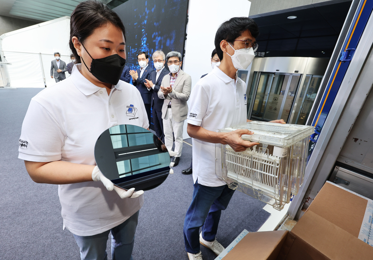
Samsung Electronics has started shipping chips produced using the world’s most advanced 3-nanometer manufacturing technology, which has drastically improved power consumption and performance.
On Monday, the tech giant held a ceremony to celebrate the departure of the first batch of 3nm chips from its chip-making complex in Hwaseong, Gyeonggi Province, with some 100 company and government officials in attendance.
The 3nm technology is Samsung’s secret weapon to outpacing its rival TSMC. Despite its prowess in memory chips, Samsung remains a distant No. 2 in the burgeoning foundry market with less than 20 percent share, with TSMC dominating more than 50 percent of the global market.
Samsung’s 3nm technology boasts higher transistor density than the current 5nm technology, which means higher speed and lower power consumption of advanced chips for artificial intelligence, big data and autonomous cars.
Samsung is also the first to adopt a more advanced transistor architecture, called gate-all-around field-effect transistor technology (GAAFET), which has increased the overall efficiency of the current fin field-effect transistor technology (FinFET).
Samsung trademarked its own GAAFET technology as “Multi-Bridge-Channel FET (MBCFET).”
GAAFET is considered essential for next-generation foundry microfabrication, which is smaller than 3nm, but chipmakers are struggling to elevate the low yield rate in the earlier stage of the production.
According to Samsung, its engineers started research work on the GAAFET technology in the early 2000s and adopted the technology for the then upcoming 3nm manufacturing process from 2017. Last month, the company made the mass production of the 3nm chips official, becoming the first chipmaker to do so.
“The latest 3nm production is a milestone for Samsung’s foundry business,” Kyung Kye-hyun, CEO of Samsung’s chip business division, told researchers at the event. “At a time when the FinFET technology is nearing its limits, we have succeeded in developing the GAAFET technology as an alternative earlier than others. This is an outcome of innovation.”
As a result of overall technological upgrades, Samsung said its first-generation 3nm process has reduced power consumption by 45 percent and improved performance by 23 percent, compared to the current 5nm process using FinFET.
For the second generation, power consumption is expected to be cut in half, with performance being boosted by 30 percent.
Samsung is adopting the latest technology to chips for high performance computing first and plans to diversity the application in partnership with clients.
The company added it is considering ramping up production to produce the chips at its other chip-making complex in Pyeongtaek, Gyeonggi Province.


![[KH Explains] Hyundai's full hybrid edge to pay off amid slow transition to pure EVs](http://res.heraldm.com/phpwas/restmb_idxmake.php?idx=652&simg=/content/image/2024/04/18/20240418050645_0.jpg&u=20240418181020)

![[Today’s K-pop] Zico drops snippet of collaboration with Jennie](http://res.heraldm.com/phpwas/restmb_idxmake.php?idx=642&simg=/content/image/2024/04/18/20240418050702_0.jpg&u=)