
Most Popular
-
1
1 in 3 Koreans live alone, family types becoming diverse

-
2
Korea, Japan finance chiefs vow to tame rampant FX market volatility

-
3
US 'incredibly concerned' about suspected NK-Iran military ties

-
4
K-pop group's manager dismissed for setting up spycam in theater dressing room

-
5
K-pop singer lost consciousness after being hit by foul ball, cancels show


![[Kim Seong-kon] Democracy and the future of South Korea](http://res.heraldm.com/phpwas/restmb_idxmake.php?idx=644&simg=/content/image/2024/04/16/20240416050802_0.jpg&u=)


[Chew on IT] Samsung chips vs. SK hynix chips: How do they fare against each other?
The Korea Herald looks at advancements in chip manufacturing technologies, past and present
By Song Su-hyunPublished : Feb. 19, 2020 - 17:12
As of the third quarter of last year, the combined market share of the two Korean chipmakers for DRAM, worldwide, stood at 74.4 percent, according to data from market researcher TrendForce. For NAND flash, together they accounted for 45.2 percent of the global market.
But not everyone has a clear understanding of the product details that enabled these Korean chipmakers to gain an edge in the global semiconductor race, largely due to the complexity of chipmaking technologies.
So The Korea Herald took a look at the advances Samsung and SK hynix have made in chip manufacturing technologies over the years. Where do they stand now, and what are the most cutting-edge memory products expected this year?
Neck-and-neck DRAM tech
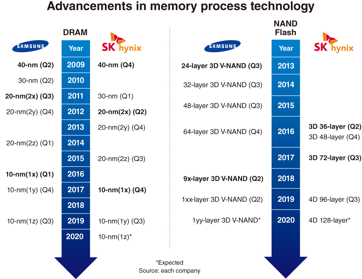
Year after year for the past decade, both Samsung and SK hynix have reached milestones in the development of their memory process technologies, migrating from a 40-nanometer process to a 10-nanometer process.
The nanometer is a unit of length equal to one-billionth of a meter, and the number of nanometers is one of the key technological specifications in semiconductor fabrication.
It is a measure of how tightly the manufacturer can fit the components on each chip -- the smaller the number, the smaller the chip. As well as bulk, being smaller is a prime determinant of the power efficiency of chips in electronics.
Both of these Korean companies took major technological leaps, particularly between 2016 and 2019.
Samsung launched the third generation of 20-nanometer-class DRAM chips in 2016. By the first quarter of 2019, Samsung had announced the third generation of 10-nanometer-class DRAM chips.
SK hynix was a couple of years behind, announcing its first generation of 10-nanometer DRAM chips in the fourth quarter of 2017. By that time, Samsung was commercializing the second generation of chips in the 10-nanometer class.
Taking a solid lead in the technological race, Samsung occupied a 45.7 percent share in the global DRAM market in the third quarter of 2019.
While Samsung is scheduled to roll out large-storage DRAM on its third-generation 10-nanometer process technology this year, SK hynix is planning to catch up soon.
“For DRAM, the technological gap between the two manufacturers has been narrowed down to less than one year, being around eight to 10 months,” said an industry official.
Fancier NAND chips
If nanometers matter for DRAM, layer numbers do for NAND flash chips.
The number of layers for NAND means how many layers of memory cells are stacked in a three-dimensional chip structure. NAND flash chips are often likened to buildings with multiple floors. Using more layers is a way of getting more capacity in the same amount of space.
Samsung started producing 24-layer NAND chips under its brand name 3D V-NAND in the third quarter of 2013. Each year, the tech giant added more layers, reaching 64 layers by the end of 2016.
SK hynix made its foray into the NAND market in 2016.
The company launched its first 36-layer NAND in the 3D structure in the second quarter of 2016. In the same year, the chipmaker stacked 12 more layers.
Then in 2017, SK hynix beat its rival to the punch by rolling out 72-layer NAND products in the third quarter.
Considering that SK hynix was about three years behind Samsung in getting into the NAND market, that quick technological advance strengthened the Korean chipmaker’s foothold in the overall memory market, industry watchers say.
SK hynix made another breakthrough for NAND technology by announcing the industry’s first 4D 96-layer NAND structure in the third quarter of last year. It is currently preparing to churn out 4D 128-layer products this year.
In the meantime, Samsung seems to have changed its NAND strategy.
The company decided not to reveal the number of layers in 2018 as it announced the 9x-layer 3D V-NAND. The term 9x means over 90 layers.
Going beyond the competition, Samsung subsequently introduced its 1xx-layer NANDin 2019 and is planning to announce a 1yy-layer NAND this year.
The change in the naming of NAND products is seen as a crucial tactic aimed at sprucing up the latest NAND technology while covering technological challenges faced by the chipmakers.
“As electronics get even smaller these days, a technological challenge is to stack over 100 layers,” an industry source said. “Some say that Samsung’s upcoming 1yy-layer NAND would have about 190 layers, but you never know if it’s really 190 layers. In most cases, fewer layers would be stacked when actually going into devices.
“Although the exact number of layers is not released as public information, customers would notice and they do discuss the product specs,” he added.
Next-generation memory
For NAND, both chipmakers are refraining from the “stacking” competition, while trying to seek technological breakthroughs to reduce the volume of the high-rise memory chips but with the same data processing and storage performance.
For DRAM, it seems like the companies are still striving hard to go lower than the 10-nanometer class.
After the 1z process (the third generation of 10-nanometer-class chips) both Samsung and SK hynix are planning to develop the fourth generation, called “1a.”
Samsung recently set up a road map for the new generation of DRAM for the new process, which will also require using extreme ultraviolet lithography technology in the next few years.
“Breaking further down below the 10-nanometer class will take several more years as nanometer process technology gets far more complex than it previously did,” said a Samsung official.
SK hynix is yet to release an official timeline for the 1a process, according to the firm.
By Song Su-hyun (song@heraldcorp.com)


![[KH Explains] Hyundai's full hybrid edge to pay off amid slow transition to pure EVs](http://res.heraldm.com/phpwas/restmb_idxmake.php?idx=652&simg=/content/image/2024/04/18/20240418050645_0.jpg&u=20240418181020)

![[Today’s K-pop] Zico drops snippet of collaboration with Jennie](http://res.heraldm.com/phpwas/restmb_idxmake.php?idx=642&simg=/content/image/2024/04/18/20240418050702_0.jpg&u=)