

Most Popular
-
1
1 in 3 Koreans live alone, family types becoming diverse

-
2
Korea, Japan finance chiefs vow to tame rampant FX market volatility

-
3
US 'incredibly concerned' about suspected NK-Iran military ties

-
4
K-pop group's manager dismissed for setting up spycam in theater dressing room

-
5
K-pop singer lost consciousness after being hit by foul ball, cancels show


![[Kim Seong-kon] Democracy and the future of South Korea](http://res.heraldm.com/phpwas/restmb_idxmake.php?idx=644&simg=/content/image/2024/04/16/20240416050802_0.jpg&u=)


Higher the better? NAND memory tech competition heats up
By Song Su-hyunPublished : Nov. 12, 2020 - 16:31
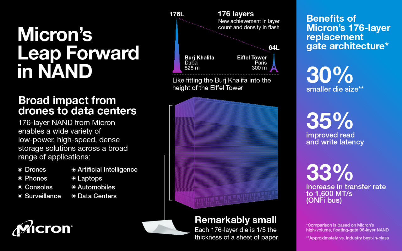
With the latest announcement of Micron’s completion of a 176-layer NAND Flash chip, pressure is mounting on market leader Samsung Electronics over its belated new product launch.
Up until early this year, it was widely expected that Samsung was going to announce the mass production of its seventh-generation 3D V-NAND Flash this year.
However, industry insider s said that the Korean chip giant seems to have changed plans due to technological challenges that it has not yet overcome.
Samsung had initially planned to introduce the new generation NAND with over 190 layers of cells, which could have been the most-layered NAND chip if the plan had gone smoothly.
“Due to unknown technological reasons, the company’s layer goal has been reduced to 176 layers,” said an industry official.
The delay in Samsung’s advancement in NAND chips suggests narrowing technological gaps between Samsung and other competitors, market watchers point out.
Samsung is rumored to have shifted from its original single-stack technology, which requires fewer processes and materials and is therefore less costly, to double-stack as it has found it difficult to stack beyond 128 layers.
“While Micron and SK hynix have been using the double-stack technology to add more layers to NAND chips, Samsung has adhered to the single-stack technology for up to 200 layers, but it seems to have realized the technological limits,” explained a source familiar to the memory technology.
The double-stack technology that puts two smaller-layer NAND chips on top of each other is deemed easier and more accessible.
Samsung refuses to confirm that its initial plan for the next generation NAND development is being delayed.
But the tech giant acknowledges that it is now behind of Micron in getting ready for announcing a new technology.
“Due to the technology shift, it would take longer time and (more) costs to transform the manufacturing processes,” a Samsung official said. “However, we are planning to introduce the next NAND product next year as scheduled.”
Along with the efforts to stack more layers on NAND chips, Samsung is also seeking technological innovation to expand the data volume per cell with high security.
While most of currently available NAND chip cells contain 3 bits, called “triple level cell” method, Samsung aims to increase the cell volume with technological breakthroughs.
“As devices get smaller and smaller, it could be impossible to raise the NAND layers further,” the Samsung official said. “The industry is striving to find solutions for that.”
SK hynix is also said to have embarked on development of a 176-layer 4D NAND Flash memory in its race to catch up with the top-tier rivals.
With the recent announcement to acquire Intel’s NAND memory unit, SK hynix is accelerating its push into the NAND market.
The Intel unit has a strong technological edge over other NAND makers, which is the quadruple level cell technology that stores 4-bit data per cell. This large-volume NAND technology is strongly preferred in the enterprise market.
As SK hynix aims to expand the proportion of its NAND business to up to 40 percent of the company’s total sales with its Intel acquisition, it could further narrow the gap between itself and market No. 1 Samsung.
According to market researcher Omdia, Samsung was the biggest NAND provider with a 35.9 percent last year, followed by Japan’s Kioxia with 19 percent, Western Digital with 13.8 percent, Micron with 11.1 percent and SK hynix 9.9 percent.
When the Intel takeover is completed, SK hynix is expected to rise to the second-biggest NAND provider in terms of market share.
By Song Su-hyun (song@heraldcorp.com)


![[KH Explains] Hyundai's full hybrid edge to pay off amid slow transition to pure EVs](http://res.heraldm.com/phpwas/restmb_idxmake.php?idx=652&simg=/content/image/2024/04/18/20240418050645_0.jpg&u=20240418181020)

![[Today’s K-pop] Zico drops snippet of collaboration with Jennie](http://res.heraldm.com/phpwas/restmb_idxmake.php?idx=642&simg=/content/image/2024/04/18/20240418050702_0.jpg&u=)