

Most Popular
-
1
1 in 3 Koreans live alone, family types becoming diverse

-
2
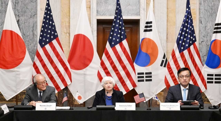
Korea, Japan finance chiefs vow to tame rampant FX market volatility
-
3
US 'incredibly concerned' about suspected NK-Iran military ties
-
4
K-pop group's manager dismissed for setting up spycam in theater dressing room

-
5
K-pop singer lost consciousness after being hit by foul ball, cancels show


![[Kim Seong-kon] Democracy and the future of South Korea](http://res.heraldm.com/phpwas/restmb_idxmake.php?idx=644&simg=/content/image/2024/04/16/20240416050802_0.jpg&u=)


Korean fabless firms turn to Samsung amid Japan risk
Over 500 fabless customers, partners pay attention to Samsung’s foundry business plans at forum
By Song Su-hyunPublished : July 3, 2019 - 17:26
Amid rising tensions between South Korea and Japan over the latter’s restriction on exports of high-tech materials to Korean chip and display makers, the country’s fabless businesses turned their attention to Samsung Electronics at a forum held in Seoul on Wednesday.
More than 500 officials from fabless and semiconductor equipment firms attended the 2019 Samsung Foundry Forum held at a hotel in southern Seoul to learn about Samsung’s foundry business plans for the year.
The number of participants shot up by nearly 40 percent this year, indicating how the high-strung Korean fabless businesses are seeking clues on how to defend against Japan’s measure. Samsung’s forum was held after its announcement to invest 133 trillion won ($113.6 billion) in the system-on-chip and foundry businesses by 2030.

Despite the upbeat atmosphere on the upcoming investments by Samsung, many industry officials discussed the expected impact of the latest Japanese restrictions on the exports of three key materials needed for chipmaking.
Regarding the issue, an official from Telechips, one of Samsung’s major fabless customers, said, “We are not concerned yet, because we believe Samsung will deal with it well.” The 20-year-old fabless company uses Samsung’s 14-nanometer and 10-nanometer foundry processes to provide chips for about 10 million automobiles.
Samsung’s Jung Eun-seung, president of the firm’s foundry division, declined to comment on the matter.
With Samsung aggressively seeking to ramp up its foundry production in order to snatch the market leader position from Taiwan’s TSMC, it seems inevitable for its foundry unit to feel the impact of Japan’s action.
Jung, in his keynote speech, instead highlighted Samsung’s latest foundry process technologies, such as the development of 3-nanometer gate-all-around early and gate-all-around plus processes that are new alternatives to the current FinFET technology. It has also completed development of the 5-nanometer FinFET process that is considered to be the last generation of FinFET.
“Samsung is also scheduled to complete the 7-nanometer EUV line in Hwaseong in September and start production next January, which can help meet our customers’ needs by offering better production infrastructure,” Jung said.
The tech giant also plans to build additional EUV lines in Pyeongtaek, Gyeonggi Province, within the next few years.
“Customers can visit our fabrication lines anytime, including the Austin fab in the US,” he said.
Under the 2030 vision to become the world’s No. 1 memory and system chip company, the Samsung foundry head pledged to expand collaboration with domestic fabless firms by opening its intellectual property assets, electronic design automation tools and outsourced semiconductor assembly test systems to customers.
By Song Su-hyun (song@heraldcorp.com)
![[KH Explains] Hyundai's full hybrid edge to pay off amid slow transition to pure EVs](http://res.heraldm.com/phpwas/restmb_idxmake.php?idx=652&simg=/content/image/2024/04/18/20240418050645_0.jpg&u=20240418181020)
![[Today’s K-pop] Zico drops snippet of collaboration with Jennie](http://res.heraldm.com/phpwas/restmb_idxmake.php?idx=642&simg=/content/image/2024/04/18/20240418050702_0.jpg&u=)