Most Popular
-
1
[Exclusive] Korean military set to ban iPhones over 'security' concerns
![[Exclusive] Korean military set to ban iPhones over 'security' concerns](//res.heraldm.com/phpwas/restmb_idxmake.php?idx=644&simg=/content/image/2024/04/23/20240423050599_0.jpg&u=20240423183955)
-
2
Korean, Romanian leaders discuss defense tech, nuclear energy
-
3
[Graphic News] 77% of young Koreans still financially dependent
![[Graphic News] 77% of young Koreans still financially dependent](//res.heraldm.com/phpwas/restmb_idxmake.php?idx=644&simg=/content/image/2024/04/22/20240422050762_0.gif&u=)
-
4
S. Korea calls on Japan to confront history amid Yasukuni Shrine visit

-
5
Yoon’s jailed mother-in-law excluded from latest parole list

![[Exclusive] Korean military set to ban iPhones over 'security' concerns](http://res.heraldm.com/phpwas/restmb_idxmake.php?idx=644&simg=/content/image/2024/04/23/20240423050599_0.jpg&u=20240423183955)

![[Graphic News] 77% of young Koreans still financially dependent](http://res.heraldm.com/phpwas/restmb_idxmake.php?idx=644&simg=/content/image/2024/04/22/20240422050762_0.gif&u=)


-
6
Hybe and Min Hee-jin, CEO of Hybe sublabel Ador, lock horns

-
7
[Pressure points] Leggings in public: Fashion statement or social faux pas?
![[Pressure points] Leggings in public: Fashion statement or social faux pas?](//res.heraldm.com/phpwas/restmb_idxmake.php?idx=644&simg=/content/image/2024/04/23/20240423050669_0.jpg&u=)
-
8
Yoo Jae-suk, Yoo Yeon-seok team up in 'Whenever Possible'

-
9
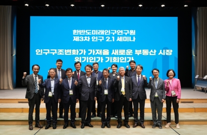
Aging population to drive down Korea's housing prices from 2040: experts
-
10
North Korea holds drills simulating nuclear counterattack against enemy


![[Pressure points] Leggings in public: Fashion statement or social faux pas?](http://res.heraldm.com/phpwas/restmb_idxmake.php?idx=644&simg=/content/image/2024/04/23/20240423050669_0.jpg&u=)


Samsung gears up for foundry with 5-nanometer EUV-based tech
By Song Su-hyunPublished : April 16, 2019 - 17:21
Samsung Electronics announced Tuesday it has completed its 5-nanometer FinFET process based on the extreme ultraviolet technology as a result of the spurred efforts to strengthen its foundry business with an aim to become the market leader by 2030.
Along with the completion of the 5nm EUV-based process, Samsung also said it will start shipping chips manufactured on the company’s 7nm process this month as the first in the foundry industry, and is aiming to start mass production of 6nm products within the year.
Along with the completion of the 5nm EUV-based process, Samsung also said it will start shipping chips manufactured on the company’s 7nm process this month as the first in the foundry industry, and is aiming to start mass production of 6nm products within the year.
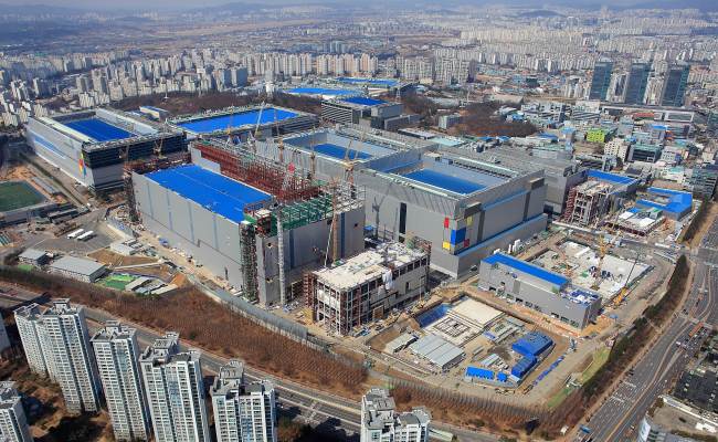
Compared to 7nm, the 5nm FinFET process tech provides up to 25 percent increase in the logic area efficiency with 20 percent lower power consumption, or 10 percent higher performance.
Like its predecessor, the 5nm technology uses EUV lithography in metal layer patterning and reduces mask layers while providing better fidelity.
The EUV lithography technology enables fabless chipmakers design highly sophisticated integrated circuits required for applications for artificial intelligence, high-performance computing, automotive systems and 5G solutions.
Another key benefit of 5nm is that customers can reuse all the 7nm intellectual properties to 5nm, enabling their transition from 7nm to 5nm with reduced migration costs, preverified design ecosystem, which will help shorten their 5nm product development, according to Samsung.
“In successful completion of our 5nm development, we’ve proven our capabilities in EUV-based nodes,” said Charlie Bae, executive vice president of Samsung’s foundry business. “In response to customers’ surging demand for advanced process technologies to differentiate their next-generation products, we continue our commitment to accelerating the volume production of EUV-based technologies.”
Samsung announced the readiness and its initial production of 7nm process, its first process node.
The company is collaborating with customers on 6nm and has already received the product tape-out of its first 6nm chip, it said.
Samsung’s EUV-based process technologies are currently being manufactured at the S3 line in Hwaseong, Gyeonggi Province. It will expand its EUV capacity to a new EUV line, which is expected to be completed within the second half of this year and start production ramp-up from next year.
By Song Su-hyun (song@heraldcorp.com)